Air quality station - Part 2
TLDR
In my previous post, I walked you through the reasons why I'm building my own air quality station and the design decisions I took.
In this post, I describe the design of the electronics and the decisions I took to arrive to the final design. I'll cover the printed circuit board (PCB) in the next post.
Intro
Having set the requirements in my previous post, it's time to work on the design of the control board.
I'll start with the "brain" of my device, the ESP32-C3-WROOM-02-H4 [1] module. Then, I'll add the connectors for the sensors and the debugging interfaces, and the glue logic around them. That's going to give me an idea of the different devices with which I need to interface, and of their supply voltages and power budgets.
With these power requirements in mind, I can determine what's the minimum capacity of the battery I'll use. Then, I'll design the power supplies and, finally, I'll focus on the design of the charger and the rest of the glue logic.
The order in which I'll design the blocks is:
Microcontroller
Connectors
Power budget and power supplies
Battery charger
Glue logic — Level translation, boot configuration, and so on.
Block design
Microprocessor
The ESP32-C3-WROOM-02-H4 module contains most of what I need to communicate with the sensors, connect to a WiFi network, and send data to the cloud.
The only external components that I need to add are a 32,768 Hz crystal for accurate timekeeping, some decoupling capacitors (C10, C11), and reset circuitry (R8, C9). According to the boot mode selection documentation [2], a C9 value of 1µF or higher should make automatic reset more reliable.
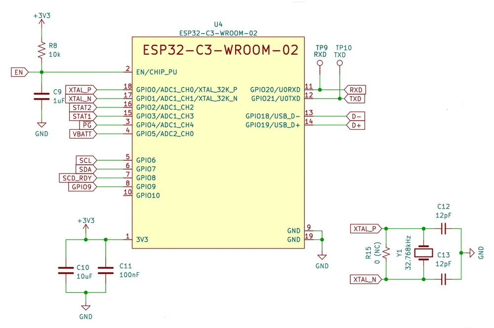
Figure 1: ESP32-C3-WROOM-02-H4 module with crystal, decoupling capacitors and reset circuit.
GPIO2 and GPIO4 are connected to the battery charger status outputs. I decided to try to see if these provide useful
information on the battery status. GPIO5 is connected to a voltage divider to monitor battery voltage.
Communication with the sensors takes place through the I²C bus, which is exposed through GPIO6 (SCL) and GPIO7 (SDA).
A third pin, GPIO8, is tied to the SCD_RDY pin of the SCD41 (CO2) sensor connector — it's there in case I
decide to try an SCD30 later on.
GPIO9 is used by the boot selector. More on this later.
GPIO20 and GPIO21 are connected to the UART pins (RXD and TXD, respectively).
And last but not least, the GPIO18 and GPIO19 are connected to the USB bus.
Connectors
USB
The USB port is wired as explained in the module datasheet [1] and as shown in the schematics of one of the development kits [3] using this module. C14 is a 4.7µF ceramic capacitor to decouple VBUS that is placed close to the USB connector.
The VBUS line sees another 1µF in parallel (C2), which is placed close to the MCP73833 battery charger IC. The total capacitance on the VBUS line is thus less than 6µF, which is well below the 10µF maximum capacitance specified by section 7.2.4.1 of the USB 2.0 specification [4].
Lastly, I added transient voltage supressor (TVS) diodes to protect the USB data and power supply (VBUS) lines from electorstatic discharge (ESD).
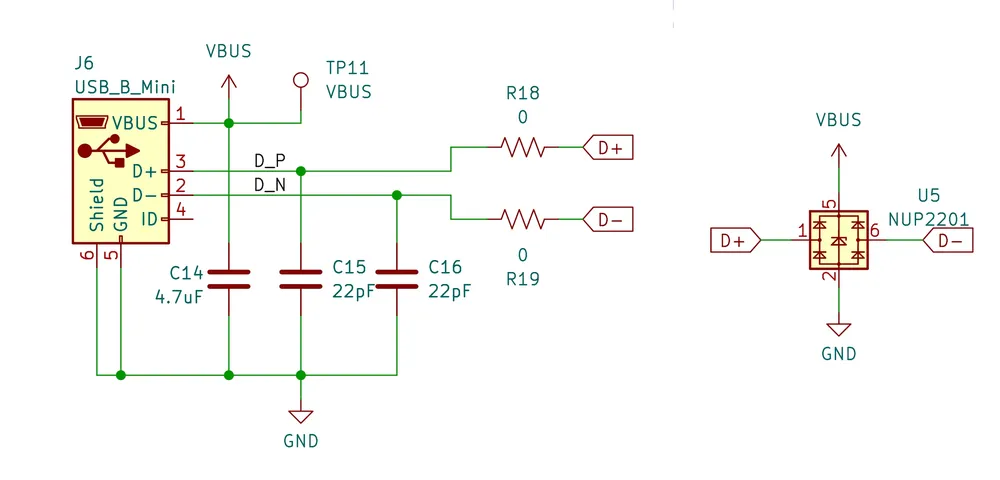
Figure 2: USB connector with TVS diodes.
UART and sensors
The rest of the connectors include a pin header to expose the UART and programming pins, and JST-XH connectors for the sensors.

Figure 3: Connectors for UART debugging and sensors.
The UART connector exposes all four lines that esptool.py needs to drive when entering the ROM bootloader mode: RXD and
TXD for communucation, and DTR and RTS to drive the EN and GPIO9 pins of the ESP32 module.
The EN and GPIO9 pins signal the ESP32-C3 which boot mode is selected [2].
All sensor connectors expose a power pin, the I²C bus, and a ground pin. The only exception is the SCD30/SCD4x connector, which
also exposes GPIO8 and is only used to read the output on the RDY (data ready) pin if an SCD30 sensor is connected.
There's a connector for an OLED display, which is optional, that also exposes the I²C bus. I'm planning to test a small 128x32 OLED display based on the SSD1306 controller.
Power budget
After listing all connectors and knowing which devices make up the air quality station, I can now work on determining the power budget.
The idea of a power budget is to know what are the current consumptions to expect on every power rail and to make sure the power supplies are properly dimensioned.
Current consumption (mA) |
|
||||
|---|---|---|---|---|---|
Device |
Idle |
Normal |
Peak |
Supply voltage (V) |
Max. power (W) |
ESP32-C3-WROOM-02-H4 |
0.13 |
82 |
345 |
3.3 |
1.13 |
SPS30 |
0.05 |
65 |
80 |
5 |
0.4 |
SCD41 |
0.5 |
18 |
205 |
3.3 |
0.68 |
BME680 |
< 1 |
13 |
18 |
3.3 |
0.04 |
OLED 128x32 SSD1306 |
< 1 |
22 |
36 |
3.3 |
0.12 |
Total |
0.68 |
200 |
604 (3.3V) / 80 (5V) |
N/A |
2.37 |
I took the estimates for the ESP32 module and the different sensors from their respective datasheets:
- ESP32 [1]
Idle — Light-sleep, typical
Normal — Active (RF working), RX, 802.11b/g/n, HT20, peak
Peak — Active (RF working), TX, 802.11b, 1Mbps, @20.5 dBm
- SPS30 [5]
Idle — Sleep mode, maximum
Normal — Measurement-Mode, maximum
Peak — Measurement-Mode, first 200ms (fan start)
- SCD41 [6]
Idle — Average supply current for periodic single shot measurement, 1 measurement / 5 minutes, maximum @ 3.3V
Normal — Average supply current for periodic measurement, maximum @ 3.3V
Peak — Peak supply current, maximum @ 3.3V
- BME680 [7]
Idle — Sleep current
Normal — Supply current during heater operation, maximum
Peak — Peak supply current
The estimates for the OLED display are from a very interesting blog post I found [8]. To know how my display fares, I'll have to measure current consumption figures myself.
Battery
If the ESP32 module and all sensors were always active and draining the battery at the rate of what the normal column states, a 2000mAh battery would deliver 2000mAh / 200mA = only 10 hours of continuous operation.
Even with a power budget, I still lack a clear understanding of how much current the device will actually use during normal operation, considering that I'm not interested in doing a continuous measurement of all parameters.
I also know that I'd like to keep the battery capacity under 600mAh for both price and size reasons.
Thus, I'll need to make as intelligent a use of the low power modes of the ESP32-C3 and the sensors as I can, and keep the average current consumption down to a minimum.
DC/DC converter
With a power budget ready, it's now time to design the power supply blocks. I'll start with the 5V supply, which I need to power my entire device from a single lithium polymer (LiPo) battery.
I'm choosing a LiPo battery because of its size and shape (small, rectangular, and flat), and because battery capacities of 600 mAh are affordable and readily available.
The usable voltage range for a standard LiPo battery ranges from 3.0V to 4.2V [20]. This means I'll need to use a boost converter [21] to deliver the 5V I need using from a lower voltage.
Being switching regulators, boost converters introduce some voltage ripple at the output, which is important to keep in mind during the design phase.
To make sure I get clean, steady 3.3V and 5V supplies, I'm choosing a boost converter that operates at a relatively high frequency, and I'm simulating the converter to have a rough idea of how it's going to behave once I build it.
Luckily for me, I had a few LMR62421X DC/DC converters in my parts box that checked all boxes. The LMR62421X can operate as a boost converter, features a fixed switching frequency of 1.6MHz and a switch current limit of 2.1A, and is compensated internally.
The total efficiency of the DC-DC converter, as estimated below, is about 88% at 200mA. The dropout of the 3.3V regulator is about 250mV, as described in the 3V3 supply seciton, which amounts to 0.25V * 0.68A = 0.17W of dissipated power.
If you're wondering how I got to this efficiency value and how did I get to choose this DC-DC regulator, I first ran a few quick simulations to understand how different ICs did at the operating conditions I established.
Thus, assuming a 30% safety margin, the peak power I need the DC-DC converter to deliver is (2.37W / 0.8 + 0.17W) * 1.4 = 4.07W. The maximum current the DC-DC converter needs to deliver is 4.07W / 5V = 0.814A ~ 820 mA.
I'm thus calculating the power supply for a maximum current of 820 mA.
I used Texas Instruments' WEBENCH Power Designer to design this block to deliver up to 820 mA of current at an input voltage of 3V, a safe cut-off voltage well above the 2.75 V discharge cut-off voltage [9] specified in the datasheet of the family of batteries I chose.
Using WEBENCH Power Designer, I also made sure the DC/DC converter operating parameters stayed well within specifications.
The decision of using the LMR62421X was not only because it was in my parts box, but because using it resulted in a very efficient (82-89%) converter over the whole range of input voltages and supply currents that I expect to see under normal operation conditions.
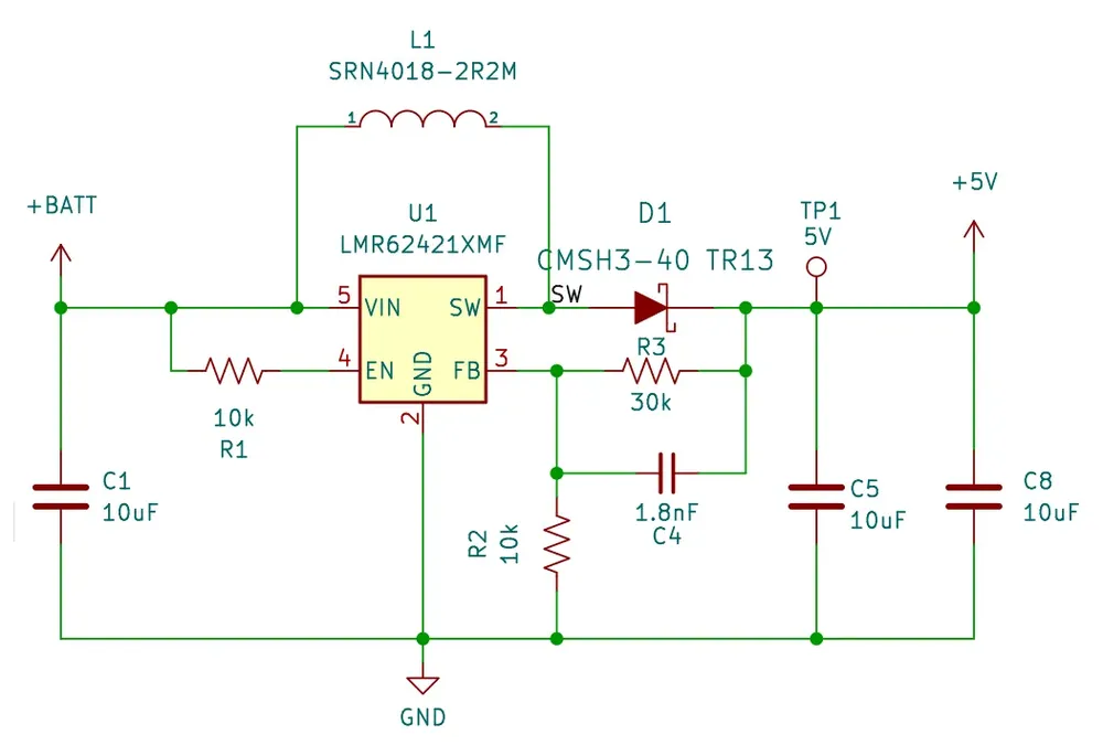
Figure 4: Block showing the DC/DC converter based on the LMR62421X IC from Texas Instruments.
The LMR62421X is enabled by pulling the EN pin up with a 10k pull-up resistor (R1). The feedback network is composed of 1% metal film resistors R2 and R3. C4 is used to compensate the converter and contributes to its stability. WEBENCH suggests a 1.8nF capacitor, but its value can theoretically be as low as 1.3nF or as high as 12nF.
The datasheet suggests capacitor C1 should be added for stability. It should be an X5R/X7R 10µF multilayer ceramic capacitor (MLCC). At the output, C5 and C8 are also MLCCs and were calculated by WEBENCH as 10µF X5R/X7R as well. Considering at least a 20% derating for capacitor voltages, 6.3V capacitors should be enough. With price not being an issue, I prefer to err on the side of caution and go for capacitors rated at 10 or 16V.
D1 is a 40V 3A CMSH3-40 Schottky diode with a 500mV forward voltage (Vf) [11]. WEBENCH recommended a diode with an average forward current of at least 2A and a recurrent peak reverse voltage (VRRM) no smaller than 7.7V, and proposed the FSV360FP [12] diode.
The FSV360FP features a higher Vf = 650mV, higher reverse current, and a recurrent peak reverse voltage (VRRM) of 60V., but is otherwise almost identical to the CMSH3-40. I went for the CMSH3-40, which I had in my parts box and should be an appropriate replacement.
Simulations
Here are some of the results of the simulations I ran. I centered on efficiency and stability of the converter, junction temperature (to understand how hot the converter would run), and the output voltage ripple.
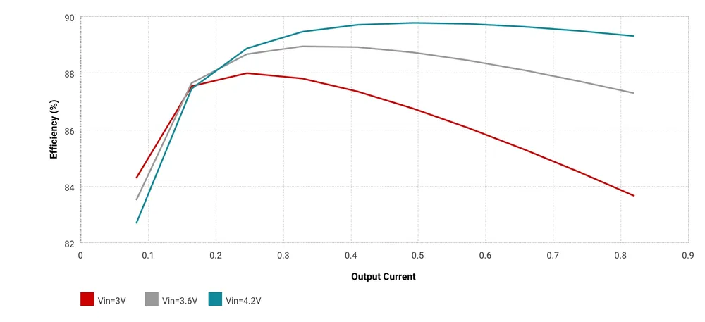
Figure 5: Efficiency of the DC/DC converter plotted against input voltage.
I'm generally happy with the efficiency figures of this particular converter. At the voltages and currents that I expect this device to work, the simulation yields excellent results. At 3V and normal operation (200 mA), the efficiency is around 88% and dropping to 84% only close to the operating limits.
Simulating the converter at lower currents, as I would expect during sleep cycles, reduces the efficiency down to 65%. At these currents, I'll have to determine whether the converter is still able to output a stable voltage. I won't find out until I build a prototype.
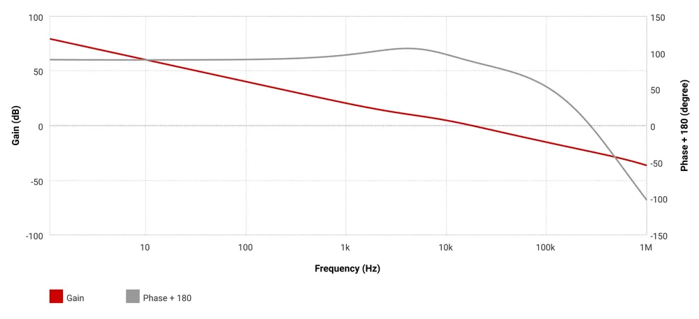
Figure 6: Loop response of the DC/DC converter
The calculated loop response for the LMR62421X in this configuration shows a stable converter, with a phase margin (87.9°) well above the minimum 45° recommended for stability [10], a crossover frequency of about 18 kHz, and a gain margin (23 dB) above the minimum 10 dB, also recommended for stability [10].
Within operating limits (3.2V – 3.9V, 10mA – 820 mA), the values the WEBENCH Power Designer calculates phase margins between 73.37° and 87.34°, a crossover frequencies between 14.67 and 16.93 kHz, and gain margins between 23.3 and 37.6 dB, which means the converter is stable across a wide range of voltages and currents.
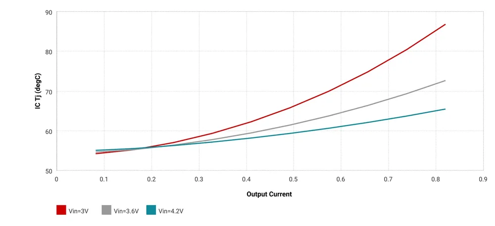
Figure 7: Junction temperature of the LMR62421X as a function of output current
At higher currents and lower input voltages, I should expect the LMR62421X to get quite hot. I may have to implement some sort of control at the software level to prevent the device from operating at lower battery voltages, both to prevent damage to the converter and to prevent the battery voltage from dropping down to its discharge cut-off voltage, which is 2.75V [9].
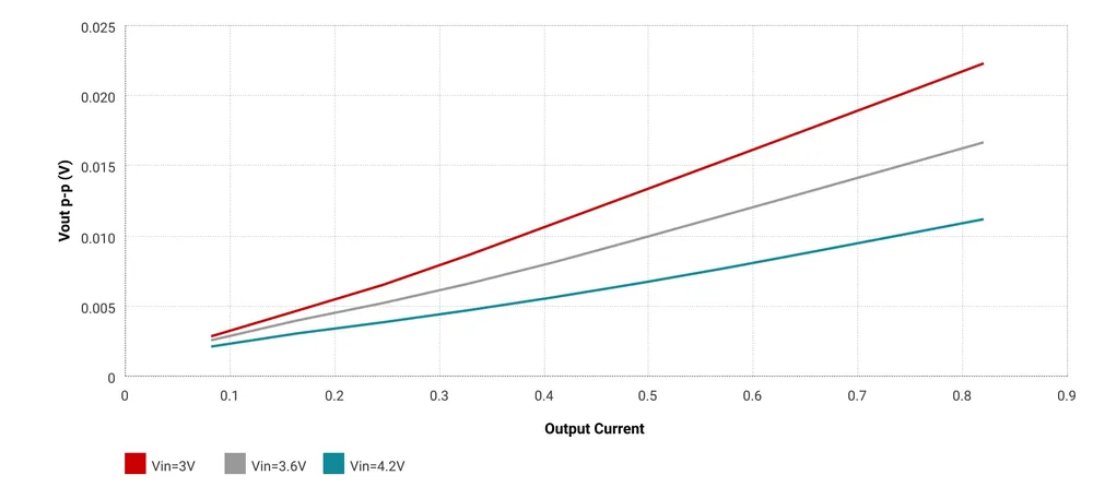
Figure 8: Output voltage ripple as a function of output current
Except when operating from a drained battery at high currents, the converter generates a very clean output with an output voltage ripple of less than 15 mVpp.
3V3 supply
To power the ESP32 module, I chose an MCP1826S linear regulator. The MCP1826S is an LDO (low dropout) regulator that can supply up to 1A of current, more than enough to supply the ESP32 and all sensors.
I chose this regulator because of its good price-performance ratio, because it's easy to solder by hand, and because it features short circuit current limiting and overtemperature protection. Its dropout voltage is also quite good (250mV @ 1A typical, 400mV @ 1A maximum).
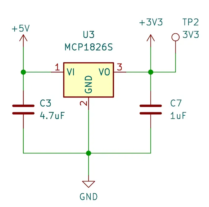
Figure 9: An MCP1826S linear regulator takes care of producing the +3.3V required to power the ESP32 module, and some of the sensors.
The design is rather simple, and mostly follows the recommendations in the datasheet.
For decoupling, both capacitors used are X7R dielectric. The 4.7µF input capacitor is rated at 16V to have ample margin for voltage spikes, whereas the output capacitor is rated at 6.3V, which means it's derated well over 60%.
Battery charger
For the battery charger, I chose the Microchip MCP73833 Li-Ion/LiPo charge management controller. I've used it in other designs before, and I chose it again because of its low cost, programmable charge current, status outputs, and small number of external components needed. I also had a few in my parts box.
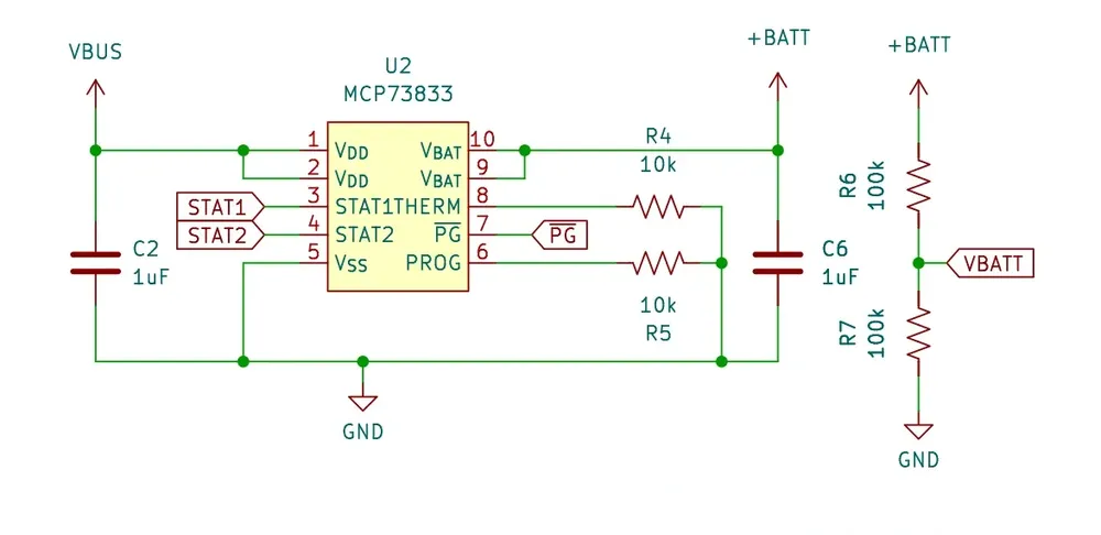
Figure 10: The battery charger, based on a Microchip MCP73833.
The design is almost identical to the reference design in the datasheet.
For this first iteration, I decided I won't be using a thermistor to monitor battery temperature, which is why the
THERM input is grounded through a 10k resistor, which tricks the charger into thinking the battery temperature
is 25°C. Using an actual thermistor is something I intend to do in future
iterations.
Logic level shifter
I used a simple MOSFET logic level shifter to communicate with the SPS30 particle sensor. If you're interested to know how it works, it's been explained multiple times, but DigiKey seems to have what I think it's the best explanation so far in their blog [13].
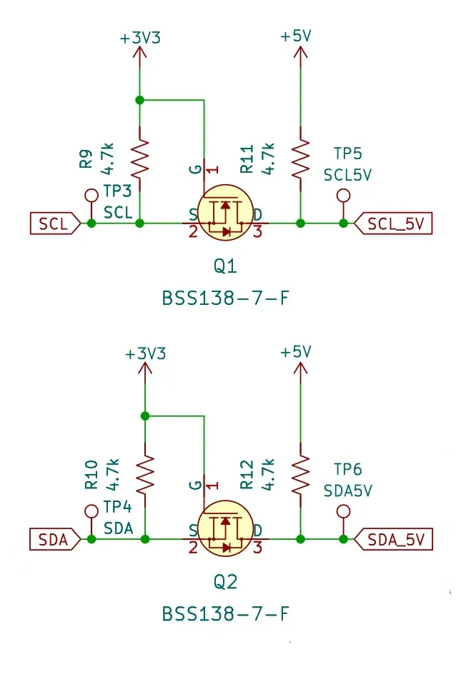
Figure 11: Logic level shifter for the I²C bus
Complete schematic
For the sake of completeness, this is what the complete schematic looks like. You'll find the OLED connector, MCP73833 status output pull-up resistors, and the boot mode selection circuit, which I omitted in the previous sections.
The boot mode selection circuit is identical to that used in ESP32 kits. This one, particularly, is identical to the one in the ESP32-C3-DevKitC-02 [3].
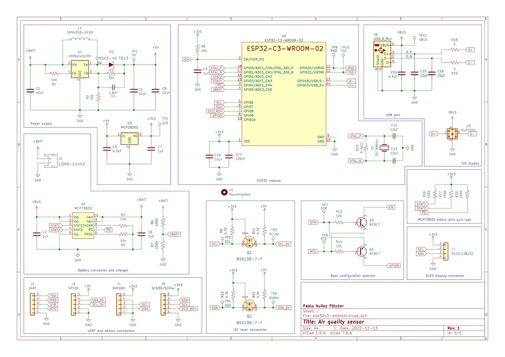
Figure 12: Complete schematics
In retrospective, I see a few things that I could've done better, and that I'm going to fix in future iterations:
Adding load sharing to the battery circuit. — I should be able to power the board from USB, if I want to. As it is today, I need to have a battery connected at all times.
Replace the MOSFET-based level shifter with a level shifter IC.
Use a MOSFET to prevent current from constantly flowing through the battery voltage divider (R6 and R7) — The current flowing through those resistors is small (4.2V / 200k = 21µA at most), but enough to reduce battery life.
Next steps
Having the schematics, it's time to work on the PCB design, send the Gerber files to a PCB manufacturer, get a few boards shipped, and start mounting the prototype. Don't forget to come back for part 3 of this series!