Air quality station - Part 3
TLDR
In my previous post, I described the design decisions I took to arrive at the monitor circuitry.
In this post, I describe the design of the printed circuit board (PCB) and the decisions I took to arrive to the final design.
Intro
I'm building a first version of the air quality monitor, so I don't expect the design to be perfect. As you will realize by the end of this post, I could've taken some better decisions. Designs can always be a bit better.
I'm not aiming at a production-grade design just yet, but at a board that will do its job while incorporating as many best practices as I can (initially) think of, and that will enable me to better understand how the circuit will behave in real-world conditions.
In the next sections, I'm presenting the different blocks and how I've laid them out. As it is by default with KiCad, red traces are on the top layer, and blue ones are on the bottom layer. Most of the bottom layer, though, is a solid ground plane.
To begin with, I'll walk you through the layout of the USB port, the battery charger and the power supply.
USB port and battery charger
The USB port is what I use both for powering the board and for debugging. It also provides the power needed to charge the battery. The MCP73833 takes power directly from the VBUS line. C2 is one of the capacitors that the MCP73833 requires for stability, which I placed as close to the IC as possible.
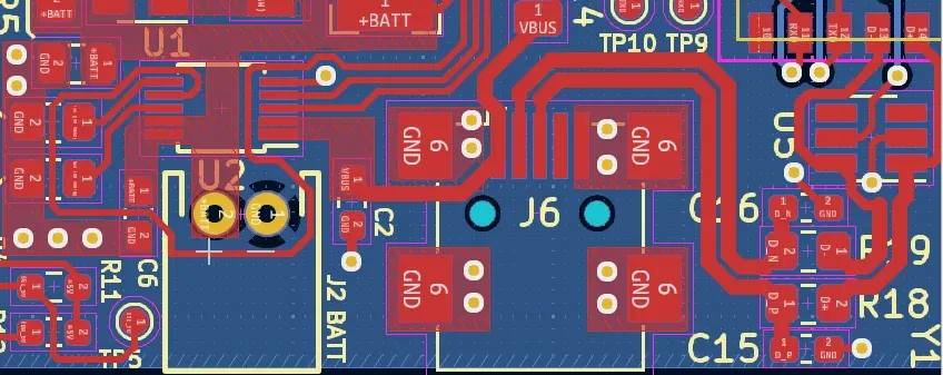
Figure 1: Layout of the Microchip MCP73833 battery charger
I routed the USB data lines trying to adhere to the USB 2.0 specification [1] to the best of my knowledge. It's not a difficult thing to do, but routing these lines right requires some prior reading to understand what the specification mandates.
The very basic requirements are:
Keep a differential impedance of 90 ohms ± 15%. This means both D+ and D- tracks need to have a specific width and track separation.
Keep the differential skew of the data lines as small as possible.
Route both lines over an unbroken ground plane.
Avoid stubs and 90-degree turns.
Avoid vias.
Following these requirements, I routed the data lines to the ESP32-C3 module over an unbroken ground plane, kept their their length matched well under 4.2mm, and used 45-degree turns everywhere I needed to bend the traces. I used no stubs or vias to route these lines, either.
To determine the width and separation of the data lines, I used the KiCad PCB calculator to get a characteristic impedance that's as close to the 90 ohms ± 15% that the USB specification mandates.
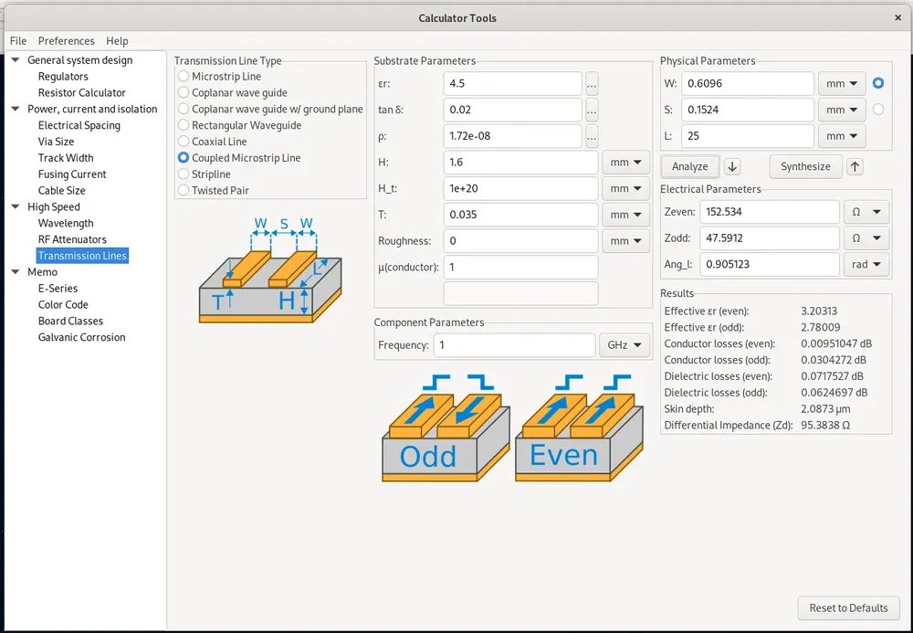
Figure 2: KiCad PCB Calculator
Using the calculator is pretty straightforward. However, the software assumes some prior knowledge, and it might not be easy to use this if it's your first time, so I'm going to walk you through it and briefly explain what each parameter means.
To begin width, there are the parameters that are related to the board itself:
εr — Relative permittivity of the substrate. This is roughly 4.5 for FR4 boards at 1 GHz.
tan δ — Loss tangent. A measure of the board material's inherent dissipation of electromagnetic energy. 0.2 for FR4 at 1 GHz.
ρ — Specific resistance. It's a copper-clad board I'm using, so this should be set to the specific resistance of copper, which is 1.72x10⁻⁸ ohms.
H — Distance to a ground plane below the trace. I'm using OSHPark's two-layer board service for this PCB [5], so this is equivalent to the thickness of the board, which is 1.6mm.
Ht — Distance to a ground plane above the trace. In this case, as there are no ground planes above the trace, Ht needs to be set to a value as close to infinity as possible.
T — The thickness of the traces. This is equivalent to the thickness of the copper. For 1oz copper, this is roughly 35µm or 0.035 mm.
Roughness — The roughness of the copper surface. It's not important to set for this particular application. I've left the default value of zero, which means the surface is perfectly smooth.
µ(conductor) — Magnetic permeability of the substrate. Not important to set for this particular application. I've left the default value of 1.
And then, there are those related to the transmission line itself:
W — Width of the tracks. I found that a 24 mil (0.6096 mm) track would be a good compromise: not too broad and yet it yielded a Zodd that's very close to the 2*Zodd = 90 ohms as possible.
S — Separation between the tracks. A 6 mil (0.1524 mm) clearance is within the capabilities of the PCB service I used and yields a Zodd that's very close to what I need.
L — Length of the tracks. This doesn't have a noticeabe effect on the impedance of the transmission lines, but it needs to be as short as possible.
Because of the size of the pins and pads of the different parts and the width of the USB tracks, I can't keep the same trace width everywhere. As long as these width changes are small and restricted to the places where they're really needed, this shouldn't be an issue.
If you're interested in the nitty-gritty details of USB signal integrity and routing, there are a few reads out there that I personally think are worth your time [2] [3] [4].
Battery charger
The layout of the battery charger isn't as demanding as that of the USB data lines. Traces need to be large enough to carry the charging current without significant ohmic loss and consequent heating.
Section 6.2 of the MCP73833 datasheet [6] briefly explains what makes a good layout, which is simply to keep the battery pack as close to the charger as possible, so as to reduce the length of the high current-carrying PCB traces. That is why the battery connector is right next to the MCP73833, and the traces are only a few millimeters long. Both input capacitors are kept nearby as well.
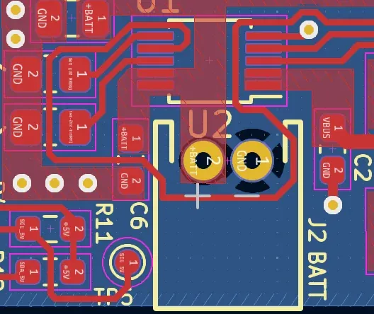
Figure 3: Layout of the Microchip MCP73833 battery charger
Boost converter
The boost converter is immediately next to the battery charger. The DC-DC converter, labeled U1, is an LM62421X in a SOT23-5 package.
According to the datasheet of the LMR62421X [7], there are a few considerations to have in mind when designing the PCB:
There must be a close coupling of the GND connections of the COUT capacitor and the LMR62421 PGND pin.
The GND ends should be close to one another and be connected to the GND plane with at least two through-holes.
There should be a continuous ground plane on the bottom layer of a two-layer board.
The FB pin is a high impedance node and care should be taken to make the FB trace short to avoid noise pickup and inaccurate regulation.
The feedback resistors should be placed as close as possible to the IC, with the AGND of R1 placed as close as possible to the GND (pin 5 for the WSON) of the IC.
The VOUT trace to R2 (R3 in our case) should be routed away from the inductor and any other traces that are switching.
The remaining components should also be placed as close as possible to the IC.
Point 3 is perhaps the easiest requirement: I've placed a solid GND plane below the LMR62421X. To meet points 4 and 5, I've placed the feedback network composed by R2, R3, and C4 as close to the feedback pin as possible. The placement of the feedback network has allowed me to also meet point 6 by routing the VOUT trace in the opposite direction of the inductor.
The GND pin is connected to the GND plane by three through-holes, which should be enough to satisfy point 2. Where I've sacrificed a little is in the placement of the output capacitors, C5 and C8, which are connected to the GND pin through the ground plane. Here, too, I'm keeping a good connection to the GND plane by using three vias.
I've tried to keep all components as close to the IC as possible, meeting point 7 to a degree I'm confident it's enough.
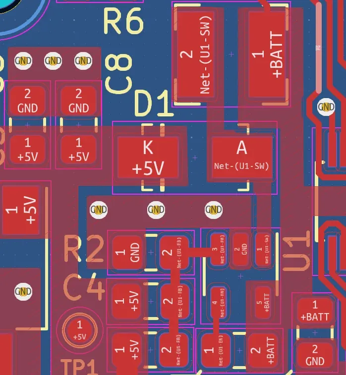
Figure 4: Layout of the boost converter. U1 is close to the lower right corner, with input capacitor C1 sitting to the right. The feedback network, composed of R2, R3, and C4 sits on its left. Output capacitors C5 and C8 are at the top right corner. The Schottky diode and inductor L1 are at the top center.
Linear regulator
The 3.3V supply, which is used to power the ESP32-C3 module and most sensors, is provided by the MCP1826S low dropout regulator.
The MCP1826S datasheet doesn't give much detail about any specific precautions for the layout. It recommends keeping the input capacitor close to the regulator, and it warns that trace resistances can cause significant power drops for high-current applications.
The latter means that it's important to keep traces wide enough to carry up to 1A of current without causing large voltage drops.
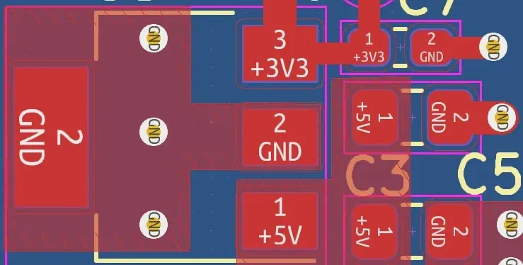
Figure 5: Efficiency of the DC/DC converter plotted against input voltage.
I provided the regulator with wide traces and a generous ground plane with stitching vias [8] to provide both a low-impedance path to the solid bottom ground and to provide some thermal relief, should the regulator get too hot.
As for the trace resistance, the narrowest trace I used for the 3.3V power rail is 24 mil wide. IPC 2221 [9] defines the maximum current a trace can carry for a given difference in temperature \(\Delta T\) as:
Where:
I is the maximum current the trace can carry, in amperes.
K is a constant that's 0.024 for internal traces and 0.048 for external traces.
\(\Delta T\) is the temperature rise above ambient in °C.
W is the width of the trace, in mils.
H is the height of the trace, in mils.
In this case, reordering the equation and solving for this particular case (W = 24, H = 1.4, K = 0.048, I = 1A), the estimated temperature rise for a 24-mil external trace carrying 1A of current is:
A 3.03°C for a 1A current is more than acceptable in this case, especially when the peak current should be at least 200 mA below that number.
Again, I used the KiCad PCB Calculator to get additional information, such as the dissipated power:
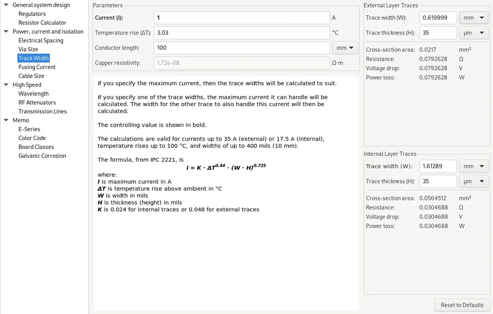
Figure 6: The KiCad PCB Calculator provides some additional useful information.
The dissipated power is 0.081 W, or 81 mW, which at 1A should be low enough.
The ESP32-C3 module
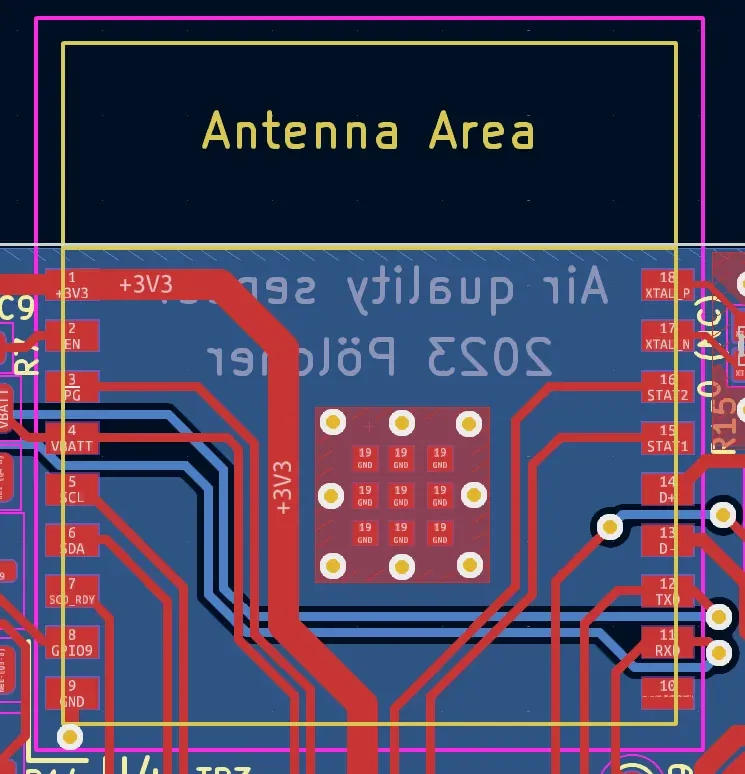
Figure 7: The ESP32C3 module
The module is relatively straightforward to place. There's a single important requirement to bear in mind, which I have seen many people simply ignore: the antenna area must be either placed off the PCB or, if you prefer, on an area of the PCB that has no ground plane (or anything at all, for that matter) beneath it.
I've provided a fairly decent ground plane on the top side of the PCB for the module and connected it using several stitching vias. The purpose is twofold: to provide a low-impedance path to the ground plane on the bottom side of the PCB, and to provide thermal relief for the module.
There's a PCB layout guide for ESP32-WROOM-02 modules [10] with other recommendations, most (if not all) of which I've addressed either locally, such as keeping filter capacitors near the regulators, or globally, such as routing traces over a solid ground plane.
The 32768 Hz crystal
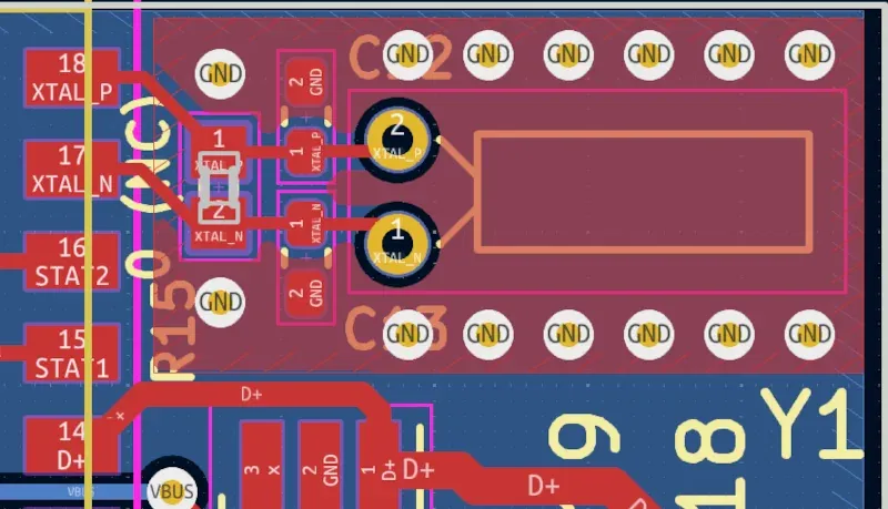
Figure 8: Routing of the traces of the 32768 Hz crystal and ground plane around it
There is a single precaution I took to route the crystal, apart from keeping traces and capacitors close. If you take a look, you can see the USB data lines routed very close to the crystal. This could introduce undesired noise into the crystal traces.
In an attempt to reduce the crosstalk, I've surrounded the crystal with a guard that's connected to the bottom ground plane through a number of stitching vias. The vias provide a low-impedance path to ground, and the ground plane beneath it should prevent the crystal case to act as an antenna.
The PCB as a whole
I won't focus on the rest of the PCB, as it doesn't anything of particular interest. A few things I think are worth mentioning are:
All connectors are placed at the edges of the PCB. Related connectors are placed next to each other. — In my opinion, this makes it easier to identify, find, and work with connectors.
The ground plane is mostly unbroken. — For this particular application, an unbroken ground plane helps with signal integrity and reduces electromagnetic interference (EMI).
Ground traces on top have plenty of vias — I've used stitching vias to provide a low-impedance path for return currents. While most of the signals present in this board are low frequency (except for the USB bus, of course), the number and type of stitching vias don't make a difference in the final cost of the PCB, don't make the design any more complex, and thus it's not a bad thing to err on the side of caution.
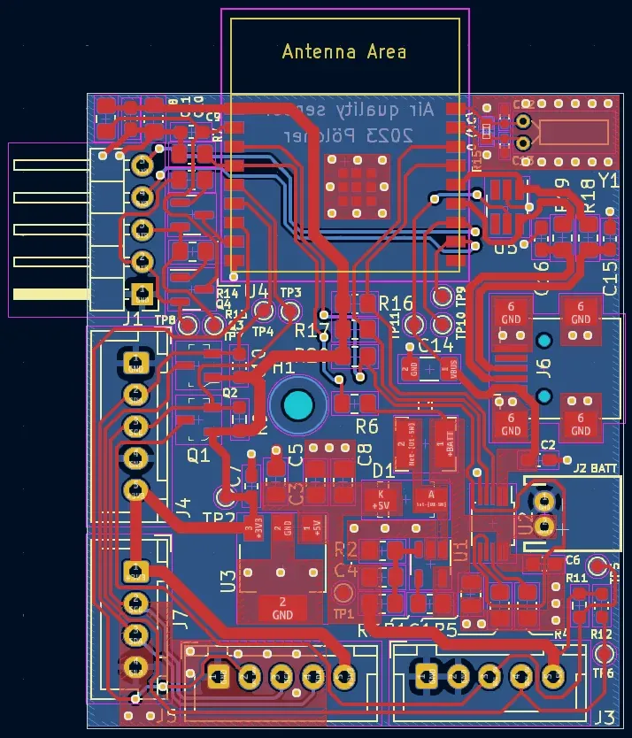
Figure 9: The whole PCB
You'll notice I've routed some of the traces on the bottom side of the PCB. I had no space left on the top side and decided to route low-speed or DC signals on the bottom side.
While it's not the end of the world, I prefer having a single solid ground pour. But, if that's not possible, signals that rise/fall slowly and DC signals with no specific requirements for noise immunity (such as a battery voltage measurement trace) are good choices for such traces.
Lessons learned
If I had to choose the thing that bugs me the most about this design is the fact that I haven't had in mind the fact that I could've OR'ed the output of the boost regulator and the USB power line. An ideal diode, such as the MAX40200 [11], would have been optimal to switch to USB power whenever the device was plugged in, while still charging the battery. You can also use a PMOS to power the circuit when an external power supply isn't connected.
An approach like this comes with the additional benefit that I'm not charging the battery and draining it at the same time, which could potentially cause the MCP73833 to miss the right conditions to stop charging.
The battery connector is a right-angle 2-pin JST-PH connector. I inadvertently placed it next to the USB connector, which turned out to be a very bad idea. This prevents me from connecting the battery and placing the USB connector right next to the enclosure wall.
I also assumed that I'd be able to work around having a single screw easily. It turned out to be a bigger issue than I initially expected, though.
While the size of the screw is quite ok, having a single point to fasten the board to the enclosure causes the board to always be tilted in one direction. The workaround is to use a small piece of plastic glued to or directly prited on the base of the enclosure that will keep the board leveled.
I initially went for a single hole to save some board space and as a challenge to get the smallest board I could, but retrospectively, it'd been wise to add those extra holes.
Finished board
All in all, the board is pretty decent. While I may go for a larger board in my next iteration, this one is good enough to start designing the enclosure and to use in a first prototype.
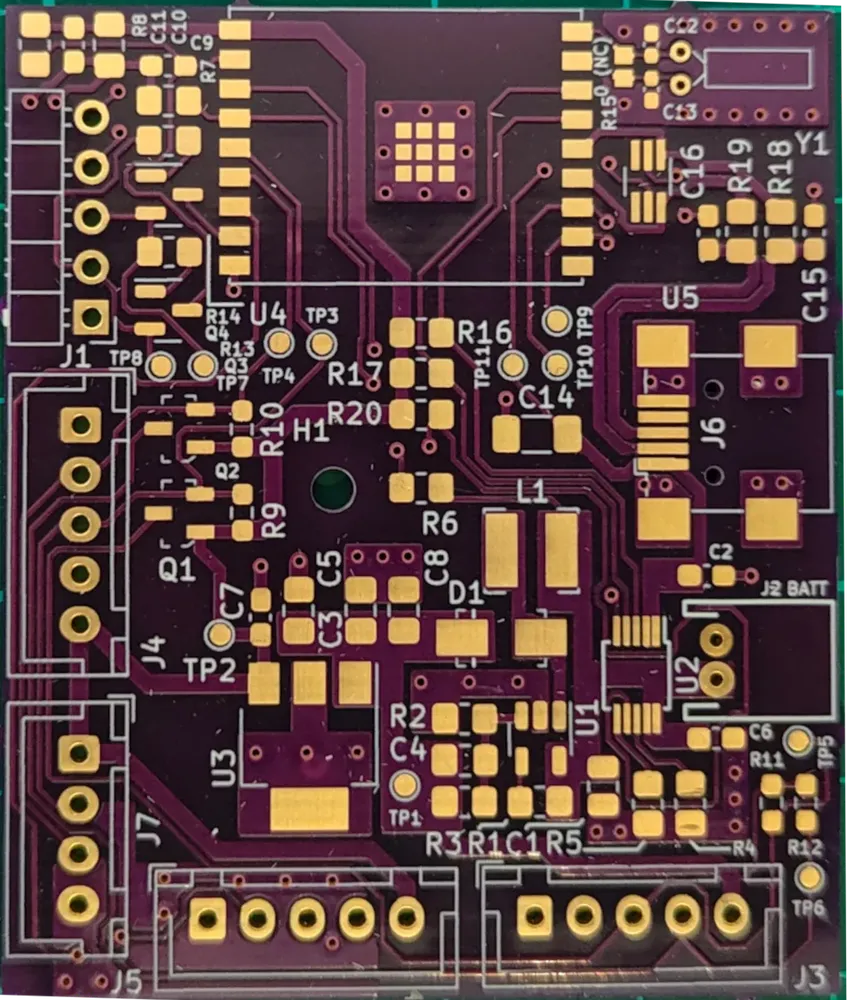
Figure 10: The end result
Next steps
As next steps, I need to write the actual firmware to get this board up and running, and I need to write the Android app to set it up, configure it, and get real-time readings from the board.
Once I'm done with it, I can start building my infra on AWS to start ingesting values through MQTT.
I'll discuss the design of a simple Android app in part 4 of this series. Don't miss it!